Connecting the debug probe to a target
The Microchip debuggers Snap and PICkit4 have an eight-pin SIL connector, where a triangle marks pin 1. This connector is not compatible with any AVR debug connector.
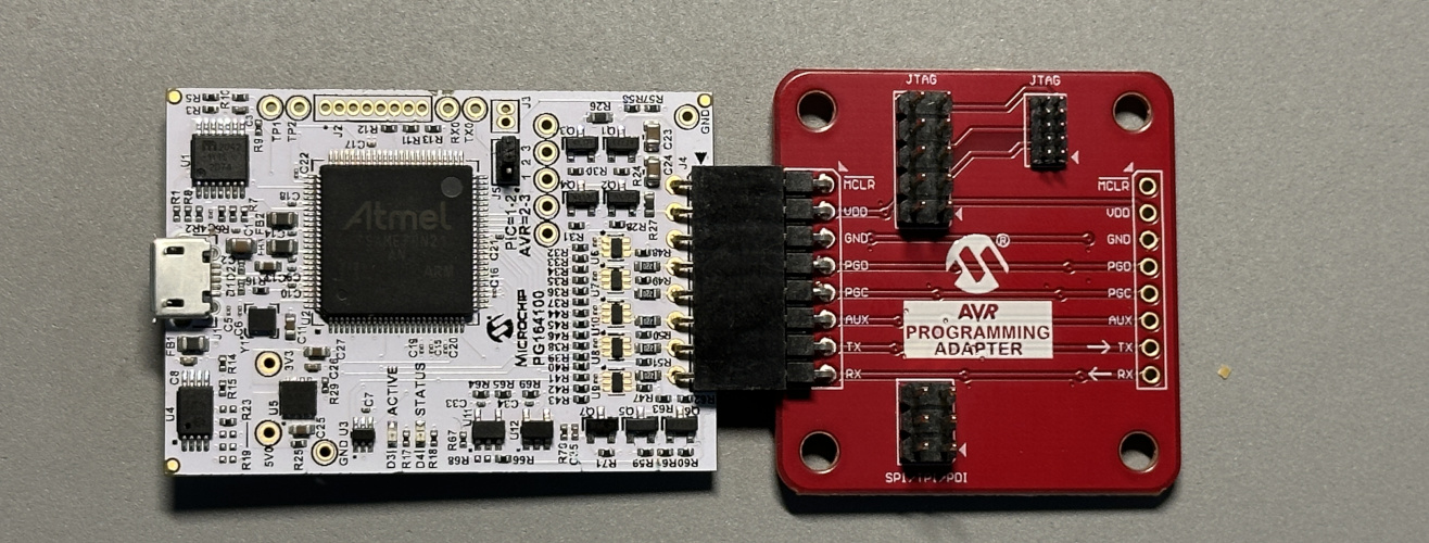
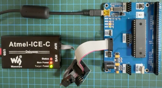
If you want to connect to your target board with a standard SPI or JTAG cable, you can buy an adapter board for AVR connectors from Microchip, as shown in the following picture.
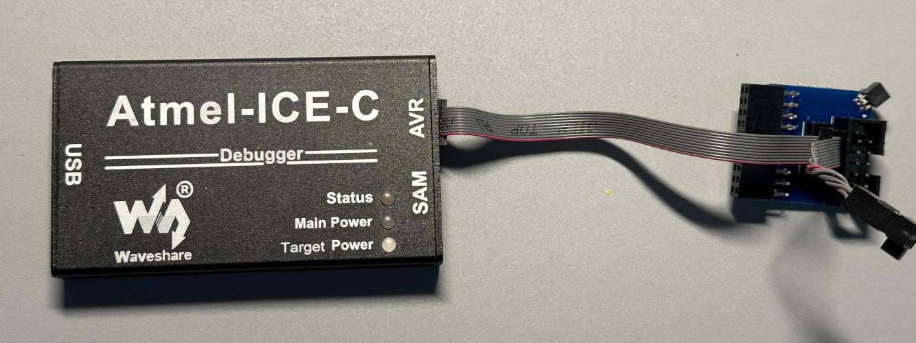
Atmel-ICE, Power Debugger, and JTAGICE3 all feature a keyed 10-pin, 50-mil JTAG header. For these debuggers, adapters are either already included or must be purchased separately. For AVR targets, one should, of course, use the header marked AVR.
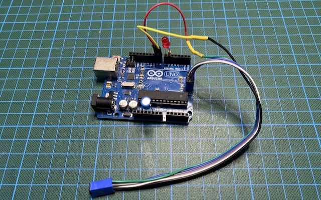
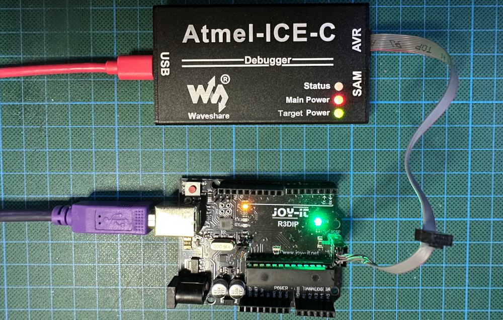
The dw-link debugger uses the header on the Arduino Uno. The most convenient way is to prepare an ISP cable with a broken-out RESET and VCC cable as shown in the the following picture.
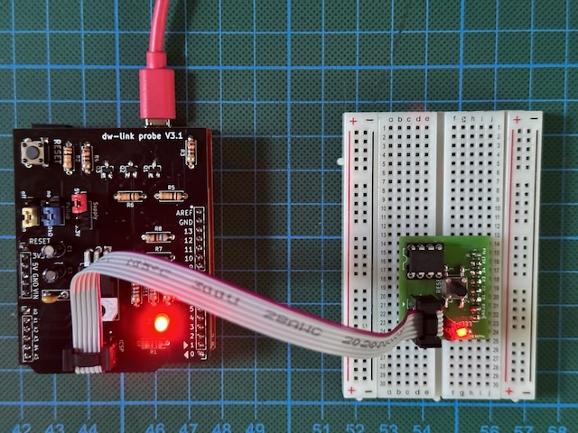
If a dw-link shield is used, one can use the standard 6-pin SPI header.
Finally, all EDBG debuggers are easy to use. Since they are embedded debuggers, the connection to the target is already on the board.
Depending on which debugging interface the target has, the target board may provide a standard debugging header for this interface. I very much prefer to work with target boards that have the appropriate debugging headers on board. Otherwise, you may easily confuse a connection, and then nothing works.
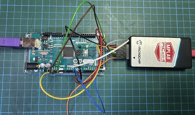
If you do not have the standard headers on board or you are using a breadboard, then you have to connect each line using a jumper cable or the Atmel squid cable, as shown in the following picture.
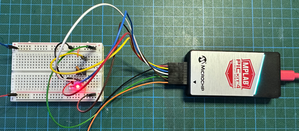
In this case, it is essential to consult the user guide of the programmer and the pinout of the MCU in the datasheet or the documentation of the respective core to make the correct connections.
Connecting to a debugWIRE target
In principle, only two wires are necessary to connect your debug probe to a target chip or board: the debugWIRE line, which is the target chip's RESET line, and GND. Since the debugger also needs to know which voltage the target board uses, the Vcc line is also necessary. Note that none of the commercial debuggers source the target. They only have voltage-sensing lines to drive the level-shifting hardware.
Since one also wants to change into and out of debugWIRE mode, change fuses, or upload firmware, it is necessary to connect all 6 SPI programming lines to the target: VTG, GND, RESET, MOSI, MISO, and SCK. For this reason, using all SPI programming lines makes a lot of sense. Moreover, most of the time, an SPI connector is already on the target board.
SPI programming header
There are two types of SPI programming connectors. The more recent type has six pins, and the older type has 10 pins, as shown in the following diagram (based on a diagram from Wikipedia, which provides a top view of the headers on a PCB.
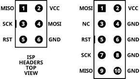
Note the notches on the left side of the headers. Since almost all SPI programming plugs are keyed, you can only plug them in in the correct orientation. However, the headers sometimes do not have notches. In this case, pin 1 is usually marked in some way, either with a dot, a star, or with the number 1. Similarly, plugs also come unkeyed. In this case, again, pin 1 is marked in some way.
Connecting to targets with an SPI programming header
If the target board has an SPI programming header, it is easy to connect to it. Simply use the SPI programming cable and plug it into the target board's header. Be aware of the correct orientation when the header is not keyed! For all the Arduino boards, pin 1 is always oriented towards the USB connector. However, if you plug it in the wrong way, nothing will be destroyed.
Connecting to targets without an SPI programming header
If the target does not feature an SPI programming header, you need to connect 6 cables. If you are working with a breadboard, you may consider buying an SPI header breadboard adapter. Otherwise, you need to connect each pin individually. Atmel-ICE, Power Debugger, and JTAGICE3 have a so-called 10-pin mini-squid cable. The pin mapping for those debuggers is as follows.
| Atmel Debugger | Mini-squid pin | Target pin | SPI pin |
|---|---|---|---|
| Pin 1 (TCK) | 1 | SCK | 3 |
| Pin 2 (GND) | 2 | GND | 6 |
| Pin 3 (TDO) | 3 | MISO | 1 |
| Pin 4 (VTG) | 4 | VTG | 2 |
| Pin 5 (TMS) | 5 | ||
| Pin 6 (nSRST) | 6 | RESET (debugWIRE) | 5 |
| Pin (N.C.) | 7 | ||
| Pin 8 (nTRST) | 8 | ||
| Pin 9 (TDI) | 9 | MOSI | 4 |
| Pin 10 (GND) | 0 |
For PICkit4 and SNAP, such a table looks as follows, with pin 1 marked by a triangle.
| MBLAP Debugger | Pin # | Target pin | SPI pin |
|---|---|---|---|
| Pin 1 (TVPP) | 1 | ||
| Pin 2 (TVDD) | 2 | VTG | 2 |
| Pin 3 (GND) | 3 | GND | 6 |
| Pin 4 (PGD) | 4 | MISO | 1 |
| Pin 5 (PGC) | 5 | SCK | 3 |
| Pin 6 (TAUX) | 6 | RESET (debugWIRE) | 5 |
| Pin 7 (TTDI) | 7 | MOSI | 4 |
| Pin 8 (TTMS) | 8 |
When you want to connect a dw-link debugger without a dw-link probe shield to a target, you can use jumper cables using the following pin mapping.
| dw-link Arduino Uno pins | Target pin | SPI pin |
|---|---|---|
| D8 | RESET (debugWIRE) | 5 |
| D11 | MOSI | 4 |
| D12 | MISO | 1 |
| D13 | SCK | 3 |
| 5V (if powered by debugger) | Vcc | 2 |
| GND | GND | 6 |
With a dw-link probe shield, it is best to construct or buy a cable with a 6-pin SPI programming plug on one end and single Dupont pins on the other.
Connecting to a JTAG target
Note that in order to use the JTAG connection, you might first need to enable the JTAG pins by programming the JTAGEN fuse via SPI programming. On chips fresh from the factory, this fuse is programmed. On Arduino boards, JTAGEN is disabled.
For AVR MCUs, there is a standard pinout as follows.
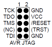
Sometimes, pin 8 is connected to nTREST, which we do not need, though. The crucial pins are TCK (JTAG clock), TDO and TDI (data lines), and TMS (control line). In addition, we have nSRST, the reset line, and VTref and GND.
Connecting to targets with a JTAG header
Again, if there is a JTAG header on the board, connecting the board is a breeze. Simply use the right cable.
Connecting to targets without a JTAG header
When debugging a program running on an Arduino Mega or Leonardo, you could use an adapter that plugs into the header, as shown in the following picture.
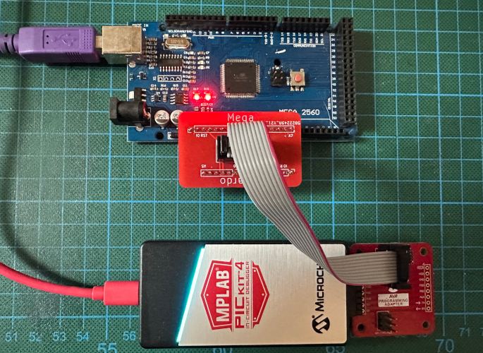
Otherwise, you must connect the wires individually, referring to the Arduino Mega's pinout and the header on the debugger. Here is an example for connecting PICkit4 (or Snap) to an Arduino Mega 2560.
The pin mapping for the PICkit4 looks as follows, where I have added the Arduino pins in the last column.
| MBLAP Debugger | Pin # | Target pin | JTAG pin | Mega pin |
|---|---|---|---|---|
| Pin 1 (TVPP) | 1 | NC | ||
| Pin 2 (TVDD) | 2 | VTG | 4 | 5V |
| Pin 3 (GND) | 3 | GND | 2, 10 | GND |
| Pin 4 (PGD) | 4 | TDO | 3 | A6 |
| Pin 5 (PGC) | 5 | TSCK | 1 | A4 |
| Pin 6 (TAUX) | 6 | RESET | 6 | RESET |
| Pin 7 (TTDI) | 7 | TDI | 9 | A7 |
| Pin 8 (TTMS) | 8 | TMS | 5 | A5 |
For the Atmel debuggers, the setup appears as follows, where the JTAG pin corresponds to the mini-squid numbering. I have additionally added the corresponding Mega pin.
| Atmel Debugger | Mini-squid pin = JTAG pin | Target pin | Mega pin |
|---|---|---|---|
| Pin 1 (TCK) | 1 | TCK | A4 |
| Pin 2 (GND) | 2 | GND | GND |
| Pin 3 (TDO) | 3 | TDO | A6 |
| Pin 4 (VTG) | 4 | VTG | 5V |
| Pin 5 (TMS) | 5 | TMS | A5 |
| Pin 6 (nSRST) | 6 | RESET | RESET |
| Pin 7 (N.C.) | 7 | NC | |
| Pin 8 (nTRST) | 8 | NC | |
| Pin 9 (TDI) | 9 | TDI | A7 |
| Pin 10 (GND) | 0 | GND | GND |
Connecting to UPDI and PDI
Will be treated later when implemented.